Today: Fri Jan 30 14:20:29 2026

I would like to warn you, if you're curious and have nothing better to do, to be careful if you want to attempt what is recorded.
It is dangerous for untrained person (sound like someone is an expert). Make your own judgement and be responsible for yourself as high voltage is dangerous.
I didn't video record when I showed my sons the power of discharging photoflash capacitor using a screen driver, a few years ago. I want to do it again and video record the event. Just another way of having some fun and at the same time, show them the power (limited though, since charge is from from capacitor) of high voltage.
So, a disposable camera of US$11 was ordered via internet. It could be a good idea to ask from photo development shop whether they have some used disposable cameras. I guess they just throw those used cameras away.
Do you ever think about how the flash light of a camera work? Ask yourself and answer to yourself before you move on. I dislike those who don't want to admit that they don't know, and will say they know it all along, after I explain to them.
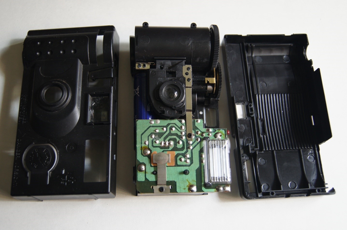
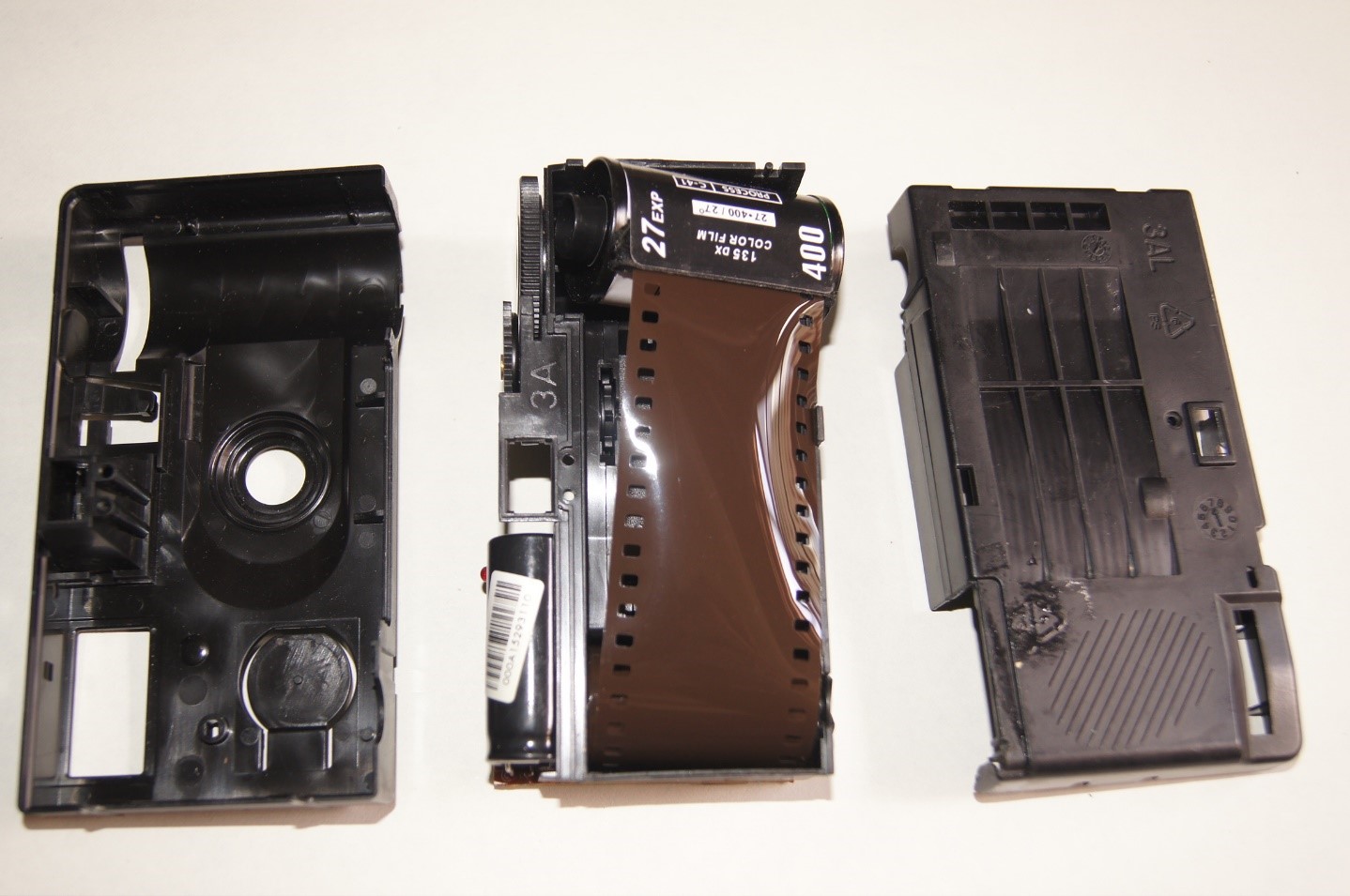
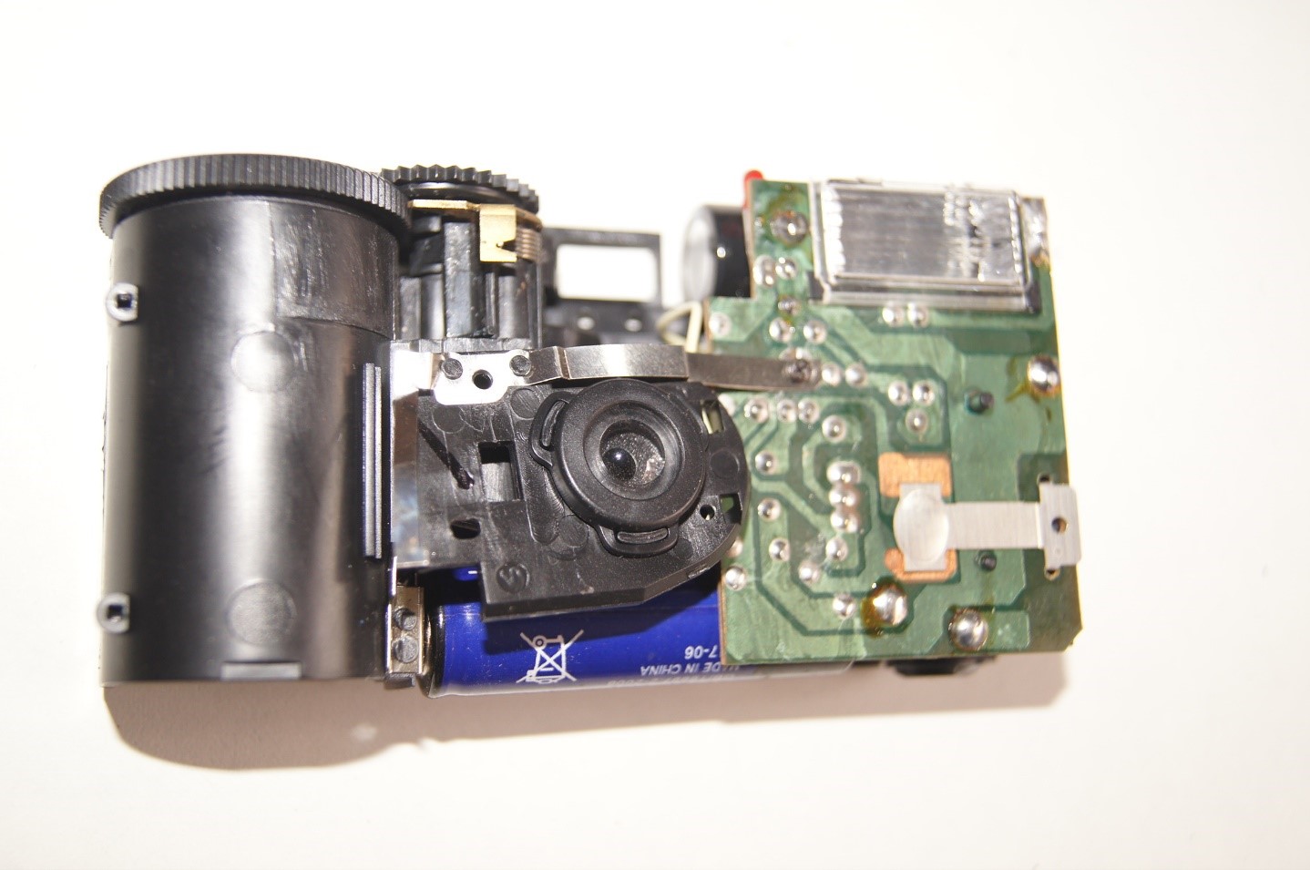
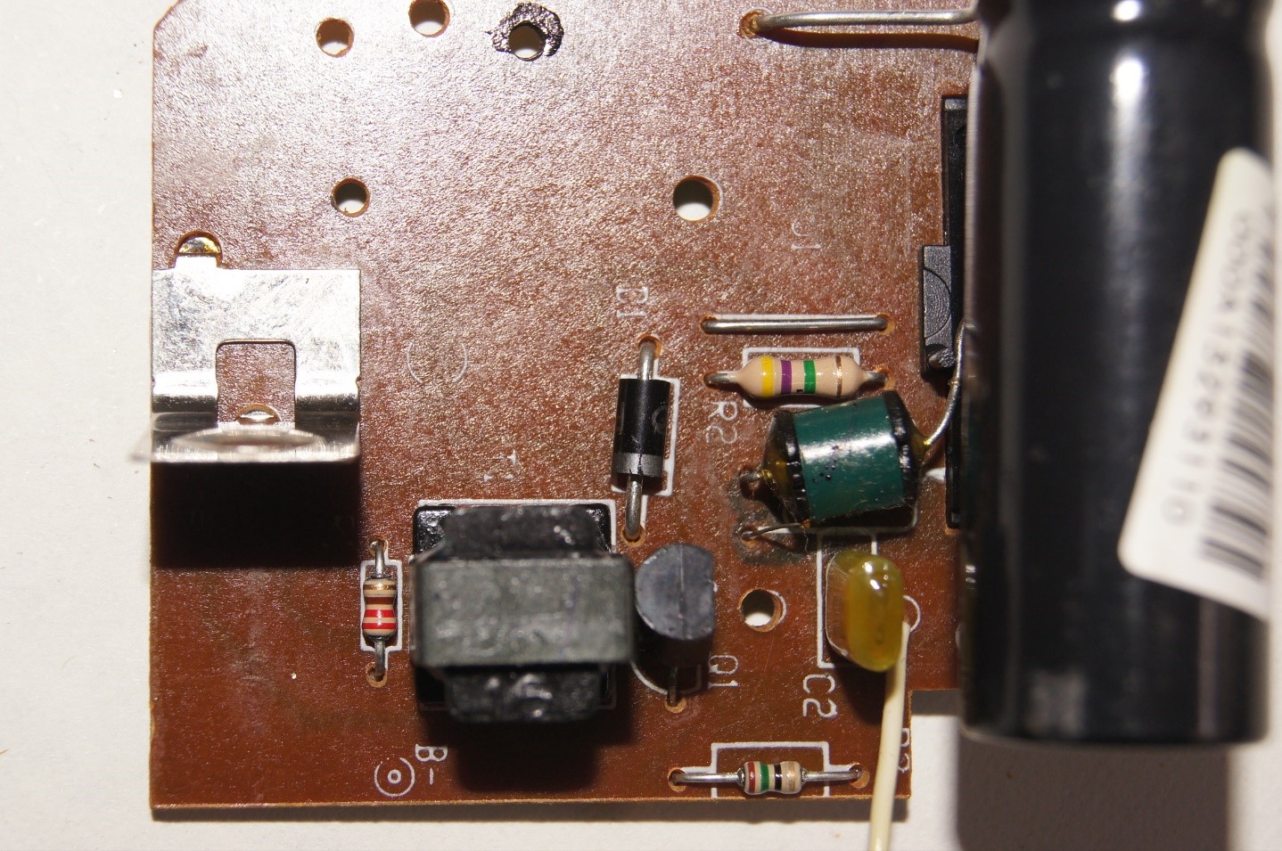
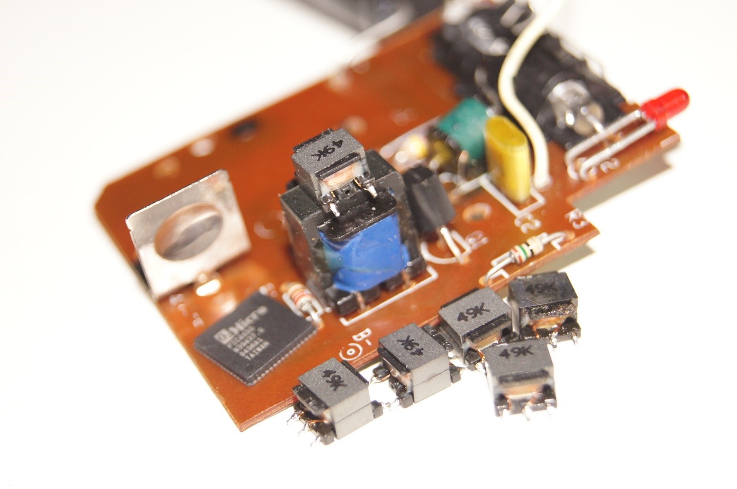
Alright, a picture is worth a thousand words. You should be able to disassemble the camera and take out the PCB.
Just make sure the camera is still functioning properly before you start the process. Remember to trigger the flash before disassembling.
After triggering of flash, the voltage left in the capacitor could be around DC 50V. Even if you touch it, it will just like an ant's bite.
However, if the capacitor is fully charged at 300V, its effect is nasty.
I still remember the experience of getting shocked by a 300V photoflash capacitor when I was doing troubleshooting of a IC project on photoflash charger.
It is nasty and you will be ok if you're not too old. The good news is that your body reaction will bounce your hand off the capacitor and your finger will leak some amount,
but not the full amount, of energy from the capacitor. You skin resistance is also unlikely to cause too much discharge of current.
You might get a little, little, bit of blister at your finger tip.
It could be interesting to try to charge certain value of capacitor to some amount of voltage level and see what level of shock we can received. We just have to start with small capacitance and small voltage, and ramp up the energy level incrementally. Don't go beyong the danger level. Don't pray pray if you're not sure.
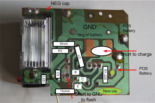
Let's assemble the camera PCB onto a bare PCB and connect the two buttons - the flash trigger button and charging button - properly. Let's do it.
It could be interesting to try to charge certain value of capacitor to some amount of voltage level and see what level of shock we can received. We just have to start with small capacitance and small voltage, and ramp up the energy level incrementally. Don't go beyong the danger level. Don't pray pray if you're not sure.
Let's assemble the camera PCB onto a bare PCB and connect the two buttons - the flash trigger button and charging button - properly. Let's do it.
I want to understand gain (since I've forgotten) how the charging circuit work, even though I have done this a couple of years ago when I worked on photoflash charger.
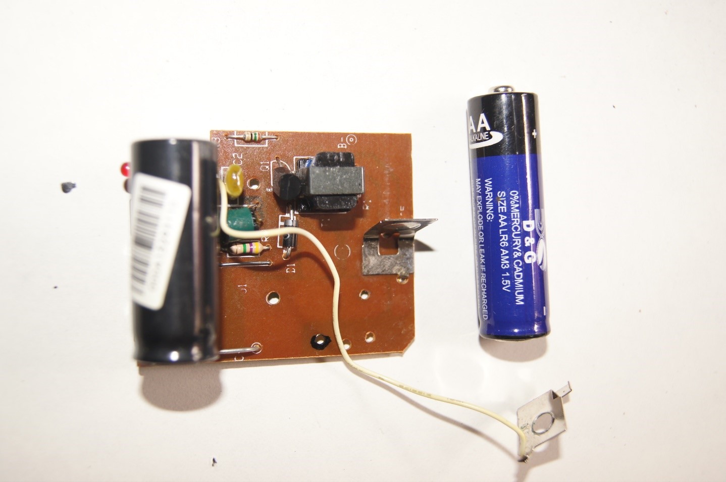
First, I took the picture of the top and bottom side of the PCB. Then, image-flip one of them so that it is easy for you to trace out the schematic with a multimeter.
Nowaday, a 'simply' grade multimeter is priced quite reasonable. I got one that cost about S$70 5 years ago and it has been since serving me well.
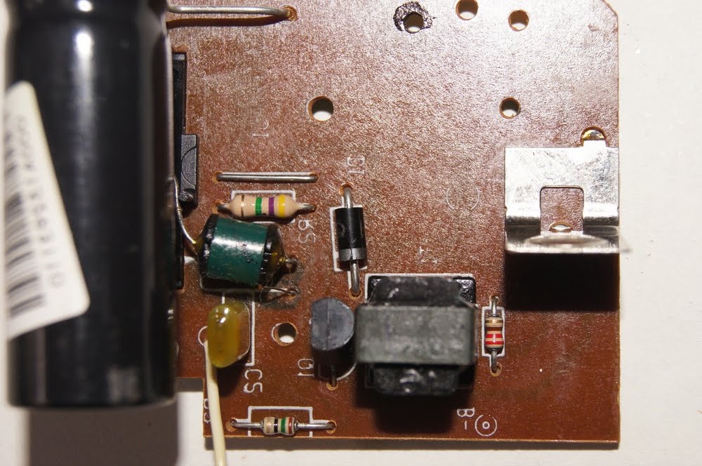
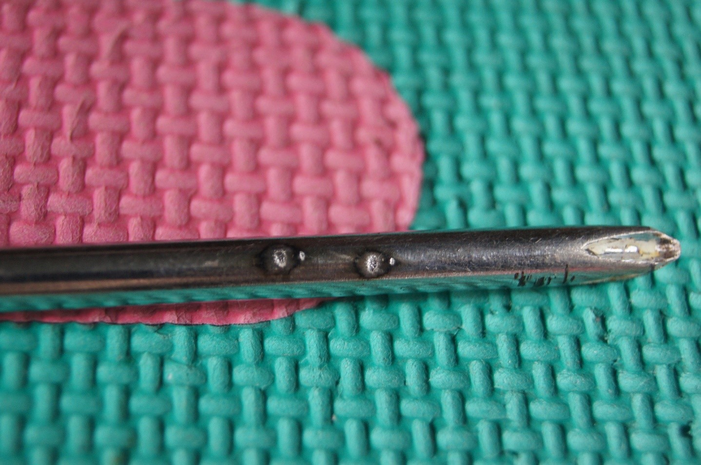
By the way, you can see the marks that are being left on the screen driver due to the high discharging current.
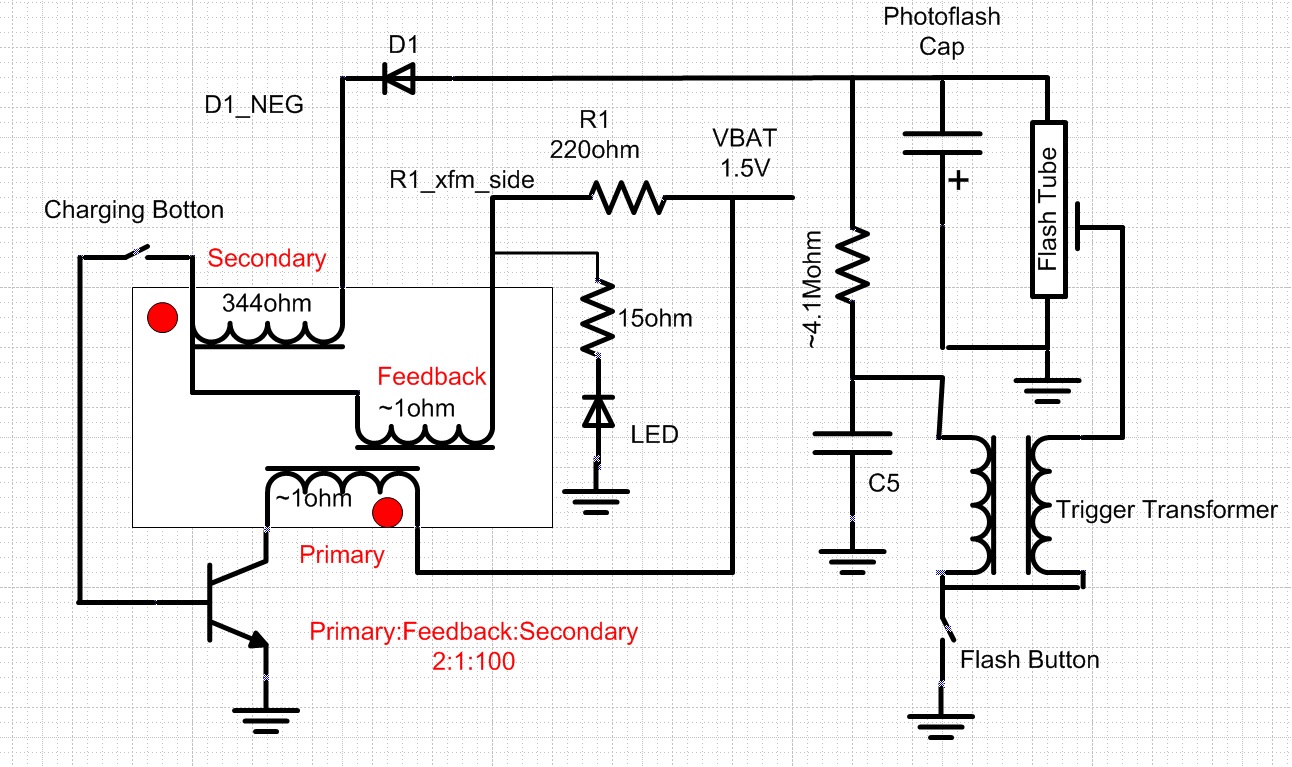
This is the circuit diagram that I reverse engineered using a multi-meter and oscilloscope. The core of the circuit is called blocking oscillator. You must remember that transformer works with only fluctuating (non-DC) current. Only changing current can produce magnetic field.
I've to admit that transformer, especially the flyback transformer, drove me nuts in the past. I'm OK with them now simply because most likely I've no more chance of crossing path with them. I've forgotten about them and I am happy not to deal with them.
OK, I'm going to try to understanding the operation. Forgive me if there are mistakes. You could drop me an email (if you have) if you discover any mistakes that I made.
Overview of Operation:
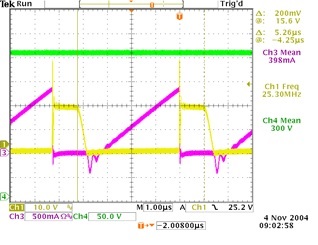
When the charging button is pressed, a small and limited (by 220Ω R1) amount of IBASE (base current) will flow into NPN BJT. The BJT will turn on finally and Ipri (primary current) start flowing in the transformer. When BJT on, the magnetizing current of primary will drive the secondary and feedback coil. Base on the polarity shown, D1 will turn on and Isec=Ipri/50 (refer to turn ratio of schematic diagram) flow into the base of BJT. This small Isec will charge the photoflash capacitor. One side of secondary coils is VBE and the other side is VD1_NEG (the negative voltage of photoflash capacitor with a forward diode voltage drop). Since BJT is on, VBE=1V and VCE=0V. As for the feedback coil, Vfeedback=(VOUT-VBE)/100~VOUT/100. When VOUT=-300V, VR1_xfm_side=VBE+Vfeedback/100=VBE-300/100=-2V, which is enough to turn on red LED.
The base current is supplied by secondary coil and feedback coil. Most of the base current is supplied by feedback coil since secondary current is lesser due to its turn ratio of 100. The base current is drawn from VBAT via R1 or LED via 15W, depending on voltage of VR1_xfm_side, which depends on Vfeedback.
When the BJT turn on, battery voltage is impressed across primary coil. Base on Vpri=L*dIpri / dt, there will be a constant ramp of primary current. The primary current will finally saturated and stop ramping up. Once Ipri saturated (or become constant or DC), the magnetic field collapsed. Isec that is flowing through D1 will drop towards zero and D1 will turn off. Isec will continue drop towards 0, reach 0, change direction to become negative current and discharged VBE towards negative voltage. Since D1 is off, VD1_NEG (with a small parasitic capacitance) will be charged up rapidly by Isec to reach, easily, <600V (depends on amount of energy left in secondary inductance). As VBE<1V, BJT will be off. VBE will swing towards negative before it will swing back to positive voltage to turn on VBE again.
To repeat again:
When BJT on, Ipri flow. Isec will charge VOUT. Ifeedback will provide IBASE to sustain BJT in the on state.
When Ipri saturated, Isec and Ifeedback will continue to sustain BJT in the on state.
When Isec reverse direction, D1 is off, VBE is discharged and BJT turn off.
This is the circuit diagram that I reverse engineered using a multi-meter and oscilloscope. The core of the circuit is called blocking oscillator. You must remember that transformer works with only fluctuating (non-DC) current. Only changing current can produce magnetic field.
I've to admit that transformer, especially the flyback transformer, drove me nuts in the past. I'm OK with them now simply because most likely I've no more chance of crossing path with them. I've forgotten about them and I am happy not to deal with them.
OK, I'm going to try to understanding the operation. Forgive me if there are mistakes. You could drop me an email (if you have) if you discover any mistakes that I made.
Overview of Operation:
When the charging button is pressed, a small and limited (by 220Ω R1) amount of IBASE (base current) will flow into NPN BJT. The BJT will turn on finally and Ipri (primary current) start flowing in the transformer. When BJT on, the magnetizing current of primary will drive the secondary and feedback coil. Base on the polarity shown, D1 will turn on and Isec=Ipri/50 (refer to turn ratio of schematic diagram) flow into the base of BJT. This small Isec will charge the photoflash capacitor. One side of secondary coils is VBE and the other side is VD1_NEG (the negative voltage of photoflash capacitor with a forward diode voltage drop). Since BJT is on, VBE=1V and VCE=0V. As for the feedback coil, Vfeedback=(VOUT-VBE)/100~VOUT/100. When VOUT=-300V, VR1_xfm_side=VBE+Vfeedback/100=VBE-300/100=-2V, which is enough to turn on red LED.
The base current is supplied by secondary coil and feedback coil. Most of the base current is supplied by feedback coil since secondary current is lesser due to its turn ratio of 100. The base current is drawn from VBAT via R1 or LED via 15W, depending on voltage of VR1_xfm_side, which depends on Vfeedback.
When the BJT turn on, battery voltage is impressed across primary coil. Base on Vpri=L*dIpri / dt, there will be a constant ramp of primary current. The primary current will finally saturated and stop ramping up. Once Ipri saturated (or become constant or DC), the magnetic field collapsed. Isec that is flowing through D1 will drop towards zero and D1 will turn off. Isec will continue drop towards 0, reach 0, change direction to become negative current and discharged VBE towards negative voltage. Since D1 is off, VD1_NEG (with a small parasitic capacitance) will be charged up rapidly by Isec to reach, easily, <600V (depends on amount of energy left in secondary inductance). As VBE<1V, BJT will be off. VBE will swing towards negative before it will swing back to positive voltage to turn on VBE again.
To repeat again:
When BJT on, Ipri flow. Isec will charge VOUT. Ifeedback will provide IBASE to sustain BJT in the on state.
When Ipri saturated, Isec and Ifeedback will continue to sustain BJT in the on state.
When Isec reverse direction, D1 is off, VBE is discharged and BJT turn off.
BJT ON |
BJT OFF |
|
VBE |
~1V |
Negative voltage due to secondary current, first discharging, follow by charging, VBE. When VBE=1V, BJT turn on. |
VCE |
~0V |
Positive voltage. Depends on Vsecondary being reflected to Vfeedback. |
D1_NEG |
D1 on. VOUT charge to a negative (large) voltage. Ifeedback will flow into VBE to sustain turn on of BJT. |
D1 off. D1_NEG voltage depends on Isec current charging D1_NEG. |
R1_xfm_side |
VBE+Vfeedback=VBE+VOUT/100=negative voltage=1-300/100=-2V when VOUT=-300V. |
~VBAT, since no current flowing through R1. |
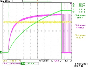
According to testing result, the charging process, will not stop when VOUT reach -310V. The operation continues since in every cycle,
there are energy loss due to BJT, D1, R1 and LED. This keeps the operation continues unless the charging button is released by the user.
During charging process, VR1_xfm_side=VBE+Vsecondary/100=1-300/100=-2V and LED is lighted up. This indicates to the user that the charging button can be released as VOUT is high enough for flashing.
The 4MΩ resistor will slowly charge C5 to VOUT. When the trigger switch is pressed, the high voltage will be impressed upon the primary coil (of the trigger transformer), and hence on the secondary coil. The high voltage, most likely >2KV will trigger the flash light.
Using blocking oscillator for photoflash charging is a simple and low cost solution that is well-suited for disposable camera. To achieve better efficiency and performance, various solutions, mostly using CMOS process technology, are available.
This is a patent that describes one solution. 7411374B2, Circuitry and control method for charging capacitive loads
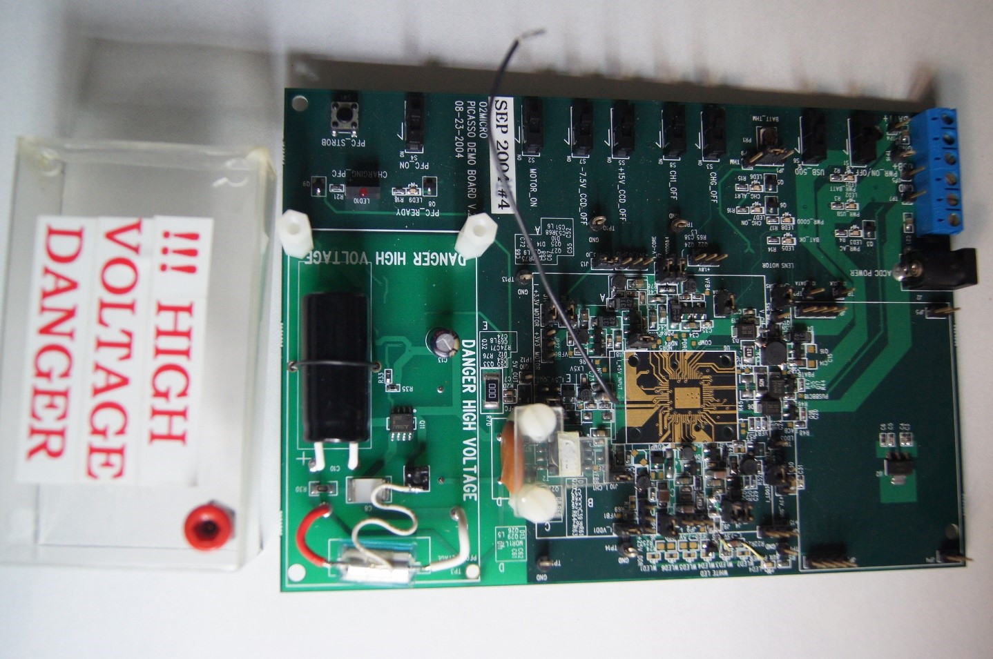
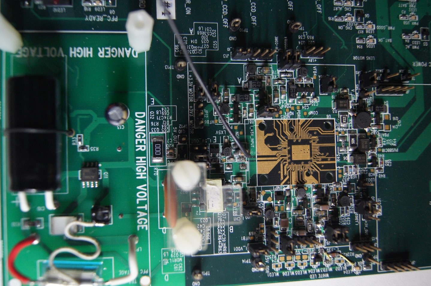
For dedicated photoflash charging IC, the control of charging are more dedicate and complex to achieve a better energy efficiency. In such case, the size of the flyback transformer used is also smaller as shown in the diagram. Depending on the status of the battery voltage, optimal charging profile can be selected.
As shown in the photographs of the evaluation test board, effort is not spared to avoid electric shock. We were very ambitious to have 12 channels of various switcing regulators, linear regulators, moter driver and etc, integrated in a power management IC, targeting for use in high end camera.
During charging process, VR1_xfm_side=VBE+Vsecondary/100=1-300/100=-2V and LED is lighted up. This indicates to the user that the charging button can be released as VOUT is high enough for flashing.
The 4MΩ resistor will slowly charge C5 to VOUT. When the trigger switch is pressed, the high voltage will be impressed upon the primary coil (of the trigger transformer), and hence on the secondary coil. The high voltage, most likely >2KV will trigger the flash light.
Using blocking oscillator for photoflash charging is a simple and low cost solution that is well-suited for disposable camera. To achieve better efficiency and performance, various solutions, mostly using CMOS process technology, are available.
This is a patent that describes one solution. 7411374B2, Circuitry and control method for charging capacitive loads
For dedicated photoflash charging IC, the control of charging are more dedicate and complex to achieve a better energy efficiency. In such case, the size of the flyback transformer used is also smaller as shown in the diagram. Depending on the status of the battery voltage, optimal charging profile can be selected.
As shown in the photographs of the evaluation test board, effort is not spared to avoid electric shock. We were very ambitious to have 12 channels of various switcing regulators, linear regulators, moter driver and etc, integrated in a power management IC, targeting for use in high end camera.
Some typical waveforms captured during the testing of the IC. That was some time ago...
Linear Technology has some solutions in this area. Just google 'linear technology photoflash charger' for their solutions. Their application notes are well-written and provide a lot of good knowledge and insight if you are working in this area.
I don't think lots of people will read in details until this point unless you have to work or study in this area. Give me a high five! For you're a determined and hardworking fellow working in a similar field as I was.
Alternatively, you might have a habit of jumping to conclusion section of a report after reading a report half way through. That is also a very smart move. You will have more chance of success compare to the 1st category of people. It is just too boring to read those - even I myself, for the >= 2nd time.
Either ways, I wish you all the best in your pursuit.